555 Timer Tutorial
The 555 Timer is a commonly used IC designed to produce a variety of output waveforms with the addition of an external RC network
We have seen that Multivibrators and CMOS Oscillators can be easily constructed from discrete components to produce relaxation oscillators for generating basic square wave output waveforms. But there are also dedicated IC’s especially designed to accurately produce the required output waveform with the addition of just a few extra timing components.
One such device that has been around since the early days of IC’s and has itself become something of an industry “standard” is the 555 Timer Oscillator which is more commonly called the “555 Timer”.
The basic 555 timer gets its name from the fact that there are three internally connected 5kΩ resistors which it uses to generate the two comparators reference voltages. The 555 timer IC is a very cheap, popular and useful precision timing device which can act as either a simple timer to generate single pulses or long time delays, or as a relaxation oscillator producing a string of stabilised waveforms of varying duty cycles from 50 to 100%.
The 555 timer chip is extremely robust and stable 8-pin device that can be operated either as a very accurate Monostable, Bistable or Astable Multivibrator to produce a variety of applications such as one-shot or delay timers, pulse generation, LED and lamp flashers, alarms and tone generation, logic clocks, frequency division, power supplies and converters etc, in fact any circuit that requires some form of time control as the list is endless.
The single 555 Timer chip in its basic form is a Bipolar 8-pin mini Dual-in-line Package (DIP) device consisting of some 25 transistors, 2 diodes and about 16 resistors arranged to form two comparators, a flip-flop and a high current output stage as shown below. As well as the 555 Timer there is also available the NE556 Timer Oscillator which combines TWO individual 555’s within a single 14-pin DIP package and low power CMOS versions of the single 555 timer such as the 7555 and LMC555 which use MOSFET transistors instead.
A simplified “block diagram” representing the internal circuitry of the 555 timer is given below with a brief explanation of each of its connecting pins to help provide a clearer understanding of how it works.
555 Timer Block Diagram
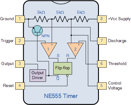
- • Pin 1. – Ground, The ground pin connects the 555 timer to the negative (0v) supply rail.
- • Pin 2. – Trigger, The negative input to comparator No 1. A negative pulse on this pin “sets” the internal Flip-flop when the voltage drops below 1/3Vcc causing the output to switch from a “LOW” to a “HIGH” state.
- • Pin 3. – Output, The output pin can drive any TTL circuit and is capable of sourcing or sinking up to 200mA of current at an output voltage equal to approximately Vcc – 1.5V so small speakers, LEDs or motors can be connected directly to the output.
- • Pin 4. – Reset, This pin is used to “reset” the internal Flip-flop controlling the state of the output, pin 3. This is an active-low input and is generally connected to a logic “1” level when not used to prevent any unwanted resetting of the output.
- • Pin 5. – Control Voltage, This pin controls the timing of the 555 by overriding the 2/3Vcc level of the voltage divider network. By applying a voltage to this pin the width of the output signal can be varied independently of the RC timing network. When not used it is connected to ground via a 10nF capacitor to eliminate any noise.
- • Pin 6. – Threshold, The positive input to comparator No 2. This pin is used to reset the Flip-flop when the voltage applied to it exceeds 2/3Vcc causing the output to switch from “HIGH” to “LOW” state. This pin connects directly to the RC timing circuit.
- • Pin 7. – Discharge, The discharge pin is connected directly to the Collector of an internal NPN transistor which is used to “discharge” the timing capacitor to ground when the output at pin 3 switches “LOW”.
- • Pin 8. – Supply +Vcc, This is the power supply pin and for general purpose TTL 555 timers is between 4.5V and 15V.
The 555 Timers name comes from the fact that there are three 5kΩ resistors connected together internally producing a voltage divider network between the supply voltage at pin 8 and ground at pin 1. The voltage across this series resistive network holds the negative inverting input of comparator two at 2/3Vcc and the positive non-inverting input to comparator one at 1/3Vcc.
The two comparators produce an output voltage dependent upon the voltage difference at their inputs which is determined by the charging and discharging action of the externally connected RC network. The outputs from both comparators are connected to the two inputs of the flip-flop which in turn produces either a “HIGH” or “LOW” level output at Q based on the states of its inputs. The output from the flip-flop is used to control a high current output switching stage to drive the connected load producing either a “HIGH” or “LOW” voltage level at the output pin.
The most common use of the 555 timer oscillator is as a simple astable oscillator by connecting two resistors and a capacitor across its terminals to generate a fixed pulse train with a time period determined by the time constant of the RC network. But the 555 timer oscillator chip can also be connected in a variety of different ways to produce Monostable or Bistable multivibrators as well as the more common Astable Multivibrator.
The Monostable 555 Timer
The operation and output of the 555 timer monostable is exactly the same as that for the transistorised one we look at previously in the Monostable Multivibrators tutorial. The difference this time is that the two transistors have been replaced by the 555 timer device. Consider the 555 timer monostable circuit below.
Monostable 555 Timer
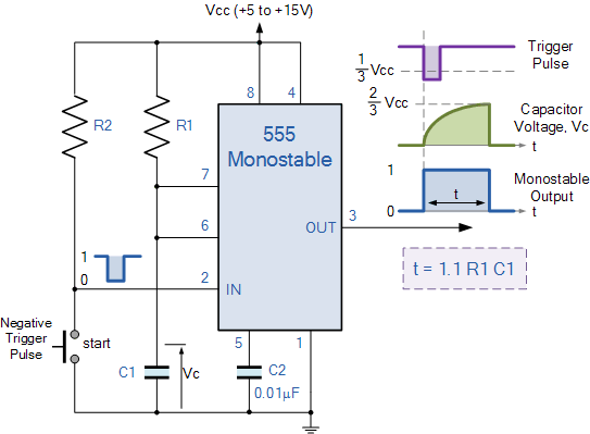
When a negative ( 0V ) pulse is applied to the trigger input (pin 2) of the Monostable configured 555 Timer oscillator, the internal comparator, (comparator No1) detects this input and “sets” the state of the flip-flop, changing the output from a “LOW” state to a “HIGH” state. This action in turn turns “OFF” the discharge transistor connected to pin 7, thereby removing the short circuit across the external timing capacitor, C1.
This action allows the timing capacitor to start to charge up through resistor, R1 until the voltage across the capacitor reaches the threshold (pin 6) voltage of 2/3Vcc set up by the internal voltage divider network. At this point the comparators output goes “HIGH” and “resets” the flip-flop back to its original state which in turn turns “ON” the transistor and discharges the capacitor to ground through pin 7. This causes the output to change its state back to the original stable “LOW” value awaiting another trigger pulse to start the timing process over again. Then as before, the Monostable Multivibrator has only “ONE” stable state.
The Monostable 555 Timer circuit triggers on a negative-going pulse applied to pin 2 and this trigger pulse must be much shorter than the output pulse width allowing time for the timing capacitor to charge and then discharge fully. Once triggered, the 555 Monostable will remain in this “HIGH” unstable output state until the time period set up by the R1 x C1 network has elapsed. The amount of time that the output voltage remains “HIGH” or at a logic “1” level, is given by the following time constant equation.
Where, t is in seconds, R is in Ω and C in Farads.
555 Timer Example No1
A Monostable 555 Timer is required to produce a time delay within a circuit. If a 10uF timing capacitor is used, calculate the value of the resistor required to produce a minimum output time delay of 500ms.
500ms is the same as saying 0.5s so by rearranging the formula above, we get the calculated value for the resistor, R as:

The calculated value for the timing resistor required to produce the required time constant of 500ms is therefore, 45.5KΩ. However, the resistor value of 45.5KΩ does not exist as a standard value resistor, so we would need to select the nearest preferred value resistor of 47kΩ which is available in all the standard ranges of tolerance from the E12 (10%) to the E96 (1%), giving us a new recalculated time delay of 517ms.
If this time difference of 17ms (500 – 517ms) is unacceptable instead of one single timing resistor, two different value resistor could be connected together in series to adjust the pulse width to the exact desired value, or a different timing capacitor value chosen.
We now know that the time delay or output pulse width of a monostable 555 timer is determined by the time constant of the connected RC network. If long time delays are required in the 10’s of seconds, it is not always advisable to use high value timing capacitors as they can be physically large, expensive and have large value tolerances, e.g, ±20%.
One alternative solution is to use a small value timing capacitor and a much larger value resistor up to about 20MΩ’s to produce the require time delay. Also by using one smaller value timing capacitor and different resistor values connected to it through a multi-position rotary switch, we can produce a Monostable 555 timer oscillator circuit that can produce different pulse widths at each switch rotation such as the switchable Monostable 555 timer circuit shown below.
A Switchable 555 Timer
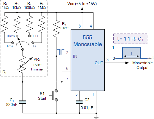
We can manually calculate the values of R and C for the individual components required as we did in the example above. However, the choice of components needed to obtain the desired time delay requires us to calculate with either kilohm’s (KΩ), Megaohm’s (MΩ), microfarad’s (μF) or picafarad’s (pF) and it is very easy to end up with a time delay that is out by a factor of ten or even a hundred.
We can make our life a little easier by using a type of chart called a “Nomograph” that will help us to find the monostable multivibrators expected frequency output for different combinations or values of both the R and C. For example,
Monostable Nomograph
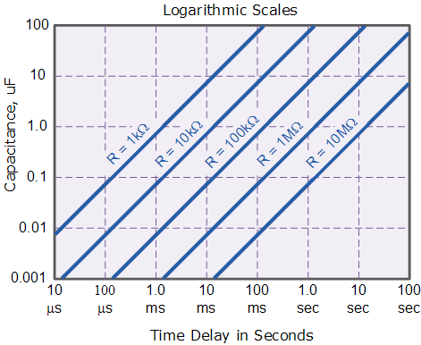
So by selecting suitable values of C and R in the ranges of 0.001uF to 100uF and 1kΩ to 10MΩ respectively, we can read the expected output frequency directly from the nomograph graph thereby eliminating any error in the calculations. In practice the value of the timing resistor for a monostable 555 timer should not be less than 1kΩ or greater than 20MΩ.
Bistable 555 Timer
As well as the one shot 555 Monostable configuration above, we can also produce a Bistable (two stable states) device with the operation and output of the 555 Bistable being similar to the transistorised one we look at previously in the Bistable Multivibrators tutorial.
The 555 Bistable is one of the simplest circuits we can build using the 555 timer oscillator chip. This bistable configuration does not use any RC timing network to produce an output waveform so no equations are required to calculate the time period of the circuit. Consider the Bistable 555 Timer circuit below.
Bistable 555 Timer (flip-flop)
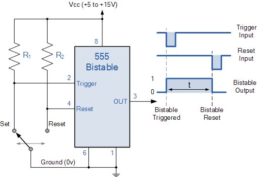
The switching of the output waveform is achieved by controlling the trigger and reset inputs of the 555 timer which are held “HIGH” by the two pull-up resistors, R1 and R2. By taking the trigger input (pin 2) “LOW”, switch in set position, changes the output state into the “HIGH” state and by taking the reset input (pin 4) “LOW”, switch in reset position, changes the output into the “LOW” state.
This 555 timer circuit will remain in either state indefinitely and is therefore bistable. Then the Bistable 555 timer is stable in both states, “HIGH” and “LOW”. The threshold input (pin 6) is connected to ground to ensure that it cannot reset the bistable circuit as it would in a normal timing application.
555 Timer Output
We could not finish this 555 Timer tutorial without discussing something about the switching and drive capabilities of the 555 timer or indeed the dual 556 Timer IC.
The output (pin 3) of the standard 555 timer or the 556 timer, has the ability to either “Sink” or “Source” a load current of up to a maximum of 200mA, which is sufficient to directly drive output transducers such as relays, filament lamps, LED’s motors, or speakers etc, with the aid of series resistors or diode protection.
This ability of the 555 timer to both “Sink” (absorb) and “Source” (supply) current means that the output device can be connected between the output terminal of the 555 timer and the supply to sink the load current or between the output terminal and ground to source the load current. For example.
Sinking and Sourcing the 555 Timer Output
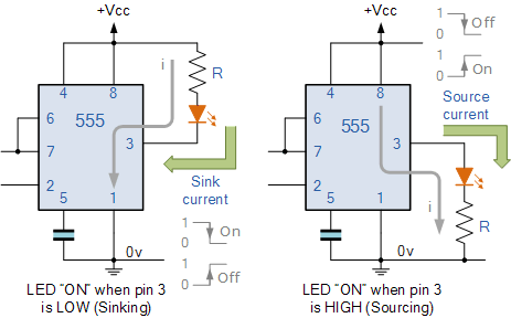
In the first circuit above, the LED is connected between the positive supply rail ( +Vcc ) and the output pin 3. This means that the current will “Sink” (absorb) or flow into the 555 timer output terminal and the LED will be “ON” when the output is “LOW”.
The second circuit above shows that the LED is connected between the output pin 3 and ground ( 0v ). This means that the current will “Source” (supply) or flow out of the 555 timers output terminal and the LED will be “ON” when the output is “HIGH”.
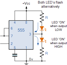
The ability of the 555 timer to both sink and source its output load current means that both LED’s can be connected to the output terminal at the same time but only one will be switched “ON” depending whether the output state is “HIGH” or “LOW”. The circuit to the left shows an example of this. the two LED’s will be alternatively switched “ON” and “OFF” depending upon the output. Resistor, R is used to limit the LED current to below 20mA.
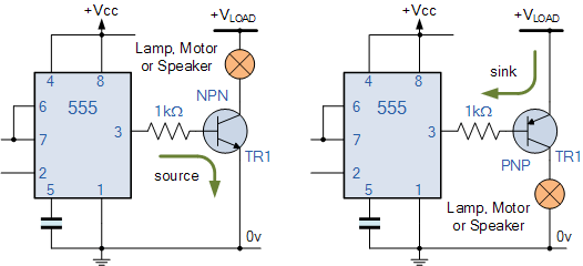
We said earlier that the maximum output current to either sink or source the load current via pin 3 is about 200mA at the maximum supply voltage, and this value is more than enough to drive or switch other logic IC’s, LED’s or small lamps, etc. But what if we wanted to switch or control higher power devices such as motors, electromagnets, relays or loudspeakers. Then we would need to use a Transistor to amplify the 555 timers output in order to provide a sufficiently high enough power to drive the load.
555 Timer Transistor Driver

The transistor in the two examples above, can be replaced with a Power MOSFET device or Darlington transistor if the load current is high. When using an inductive load such as a motor, relay or electromagnet, it is advisable to connect a freewheeling (or flywheel) diode directly across the load terminals to absorb any back emf voltages generated by the inductive device when it changes state.
Thus far we have look at using the 555 Timer to generate monostable and bistable output pulses. In the next tutorial about Waveform Generation we will look at connecting the 555 in an astable multivibrator configuration. When used in the astable mode both the frequency and duty cycle of the output waveform can be accurately controlled to produce a very versatile waveform generator.

